Figure 5.15 shows an N-channel JFET with DC bias voltage
applied.
Just as for a simple diode, the depletion region grows as the reverse
bias across the PN junction is increased, thereby constricting the
cross section of the conducting N-channel material and increasing the
resistance of the channel.
The major current ![]() in the channel is caused by the applied
voltage between the drain and source,
in the channel is caused by the applied
voltage between the drain and source, ![]() , and is controlled by
the applied voltage between the gate and source,
, and is controlled by
the applied voltage between the gate and source, ![]() .
.
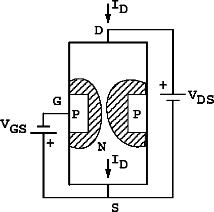
Figure 5.15: An N-channel JFET with DC bias voltages
applied.
The JFET has two distinct modes of operation: the variable-resistance
mode, and the pinch-off mode.
In the variable-resistance mode the JFET behaves like a resistor whose
value is controlled by ![]() .
In the pinch-off mode, the channel has been heavily constricted with
most of the drain-source voltage drop occuring along the narrow and
therefore high-resistance part of the channel near the depletion
regions.
.
In the pinch-off mode, the channel has been heavily constricted with
most of the drain-source voltage drop occuring along the narrow and
therefore high-resistance part of the channel near the depletion
regions.
The characteristic curves of a typical JFET are shown in
figure 5.16.
At small values of ![]() (in the range of a few tenths of a volt),
the curves of constant
(in the range of a few tenths of a volt),
the curves of constant ![]() show a linear relationship between
show a linear relationship between
![]() and
and ![]() .
This is the variable-resistance region of the graph.
As
.
This is the variable-resistance region of the graph.
As ![]() increases, each of the curves of constant
increases, each of the curves of constant ![]() enters a region of nearly constant
enters a region of nearly constant ![]() .
This is the pinch-off region, where the JFET can be used as a linear
voltage and current amplifier.
At
.
This is the pinch-off region, where the JFET can be used as a linear
voltage and current amplifier.
At ![]() the current through the JFET reaches a maximum known as
the current through the JFET reaches a maximum known as
![]() , the current from Drain to Source with the gate Shorted to
the source.
If
, the current from Drain to Source with the gate Shorted to
the source.
If ![]() goes positive for this N-channel JFET, the PN junction
becomes conducting and the JFET becomes just a forward-biased diode.
goes positive for this N-channel JFET, the PN junction
becomes conducting and the JFET becomes just a forward-biased diode.
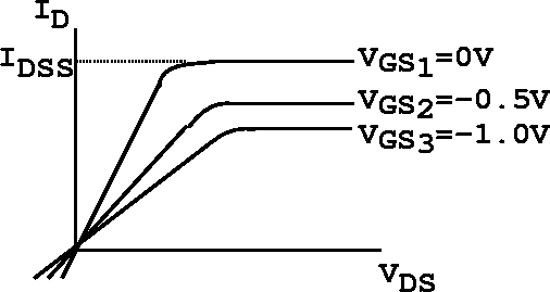
Figure 5.16: Characteristic curves of a typical N-channel
JFET.