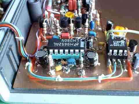
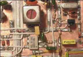
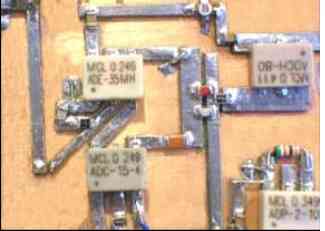
"Manhattan Style" is a technique for constructing electronic circuits by gluing pads or traces to make "islands" of separate conductivity on top of a base material. The pads or traces are cut (with a shear^ or nibbler^) or punched^ from copper clad board or thin sheets of metal ,or clipped and bent from solid wire, and affixed with super glue or other adhesive. Component leads are then soldered to the top of the pads and traces to build the circuit. A metalic base board can provide a ground plane.
Here are some examples of circuits made using Manhattan construction: (thanks to Carel Mulder - PA0CMU, and Paul Harden, na5n for permission)


Of course, if you really don't want to use a PCB, you don't have too...
Here is an Arduino made on a sheet of high temperature plastic:
http://www.edn.com/design/pc-board/4439368/Product-how-to--The-future-is-lightweight--low-cost--and-flexible
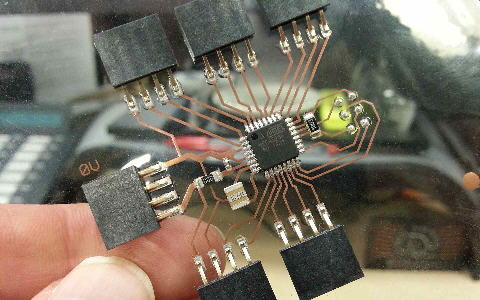
Actually, you can make a circuit on nothing at all:
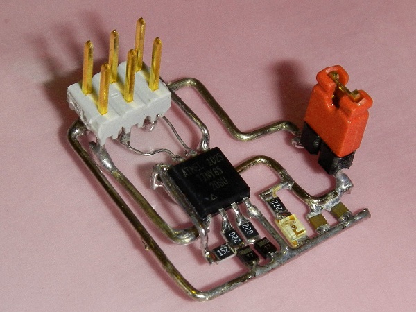
That is actually a USB AVR programmer, believe it or not.. the USB cable
hasn't been soldered on yet. More at:
http://dangerousprototypes.com/2012/10/08/little-wire-dead-bug-art/
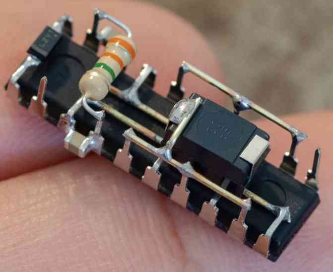
A lovely example from
https://www.linkedin.com/feed/update/urn:li:activity:6652983588708982784/
Which was apparently taken without credit from:
https://mobile.twitter.com/MohitBhoite/status/1247196505942835200
?
Here are a few pictures and descriptions to give the general idea. There are several very good tutorials listed at the bottom of the page for more detail.
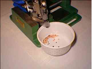 A harbor freight punch held in a vice; used to make small round
pads from copper clad board. Other methods of making pads include cutting
small square pad or long strips with a shear or PCB saw, or using a sheet
metal "nibbler"
The long strips are most useful for surface mount designs or as buss bars. Wire can also be used to connect separate smaller pads.
You can also make isolated pads in a solid PCB with spot weld drills at Harbor Freight. These drills have a spring loaded center pin that keeps the boards from wandering while you drill them. You can also drill very small pilot holes through the board to make matching pads on the opposite side of the board for feed through connections.
picture from chuck adams, k7qo used by permission
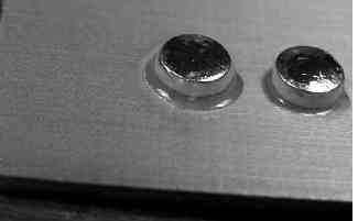 PCB
pads made from the above punch, glued to a base of copper clad board. The
tops have been tinned with solder, ready for component leads.
Care must be taken to remove any burs or "flashing" of copper that might short the top of the pad to the base ground plane. This is also important for safety.
Acetone can be used to remove the super glue holding the pads if they must be repositioned, but this can be very difficult to apply to only one pad in a tight layout, so get your pads set right before adding the components.
picture from chuck adams, k7qo used by permission
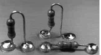 Components can be soldered vertically or horizontally between
pads or from pads to the ground plane. Notice that the ends of the leads
are always parallel with the surface they are being soldered to.
As this excellent example from chuck adams, k7qo shows, Manhattan construction can be very artistic.
picture from chuck adams, k7qo used by permission
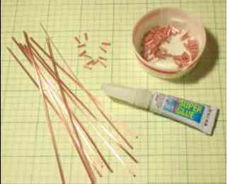 These
strips were made with a nibbler and a shear.
Super glue seems to be the best option for mounting the pads or strips on the base copper clad board.
picture from Paul Harden, na5n used by permission
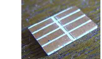 Pads for Integrated Circuits can be made by cutting away the
copper from a piece of copper clad board to make isolated segments matching
the spacing and number of pins.
picture from chuck adams, k7qo used by permission
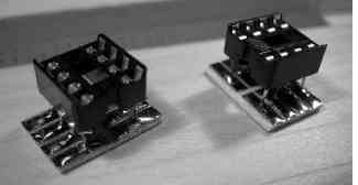 ICs can be soldered direct to pad or sockets can be used. In
either case, the leads should be bent over to provide a larger contact area
with the pad.
picture from chuck adams, k7qo used by permission
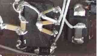 IC's can also simply be glued in place upside down and components
or wires soldered to the IC leads. This is often called "dead bug" construction.
Another option is to attach the IC right side up with a spacer under it or by soldering the leads at the corners to the regular pads as above, then bending the other leads out flat above the base PCB and soldering directly to them. One might call this "live bug" construction.
 Surface
mount is also very possible with Manhattan techniques. Note the ease of use
of through-hole components without holes as demonstrated by the resistor
in the lower right corner.
picture from Paul Harden, na5n used by permission
See also:
Questions:
| file: /Techref/pcb/manhattan.htm, 9KB, , updated: 2022/6/1 19:09, local time: 2025/6/28 05:47,
216.73.216.196,10-1-0-7:LOG IN
|
| ©2025 These pages are served without commercial sponsorship. (No popup ads, etc...).Bandwidth abuse increases hosting cost forcing sponsorship or shutdown. This server aggressively defends against automated copying for any reason including offline viewing, duplication, etc... Please respect this requirement and DO NOT RIP THIS SITE. Questions? <A HREF="http://sxlist.com/Techref/pcb/manhattan.htm"> copper clad,PCB,metal shear,metal nibbler,metal punch,soldering iron,super glue</A> |
| Did you find what you needed? |
Welcome to sxlist.com!sales, advertizing, & kind contributors just like you! Please don't rip/copy (here's why Copies of the site on CD are available at minimal cost. |
Welcome to sxlist.com! |
.