From Saurabh Gupta and Dhananjay V Gadre, Netaji Subhas Institute of Technology, Dwarka, New Delhi, India
This method allows 2×N×(N–1) LEDs using only N I/O lines and a few additional discrete components. The technique exploits the fact that each I/O line has three states: one, zero, and high impedance. Thus, with two I/O lines, states 00, 01, 10, and 11 of eight possible states control the LEDs.
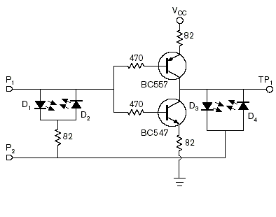
Here is an example with two I/O lines controlling four LEDs. P1 and P2 are the inputs. The circuit requires that the LED turn-on voltage should be slightly more than VCC/2. For red LEDs with a turn-on voltage of approximately 1.8V, a suitable supply voltage is 2.4V. For blue or white LEDs, you can use a 5V supply voltage. For N I/O lines, this technique requires N–1 transistor pairs.

Here are the states of P1 and P2 as they relate to which LED lights up:
| P1 | P2 | TP1 | LED |
| 0 | 0 | Vcc | D3 |
| 0 | 1 | Vcc | D2 |
| 1 | 0 | 0 | D1 |
| 1 | 1 | 0 | D4 |
| Z | Z | Vcc/2 | None |
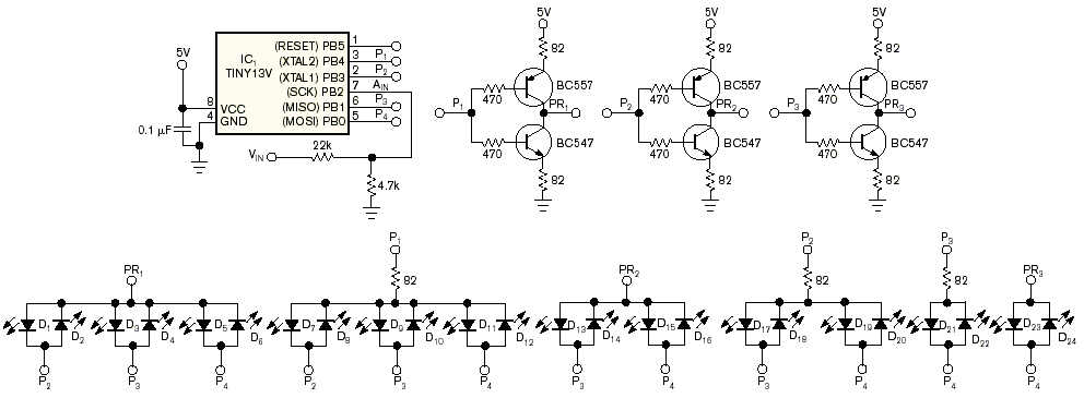
A second example shows 24 white LEDs with 4 IO pins and 6 transistors controlled by an ATMEL AT Tiny 13 Microcontroller.

And here is the C source code for a bargraph display with the analog input comming into PB2 (pin 7, Ain).
/*Saurabh Gupta and Dhananjay V. Gadre*/
/*Tiny13 Processor*/

/* January 2008*/

#include<avr/io.h>
#include<avr/interrupt.h>
#include<avr/pgmspace.h>

typedef unsigned char u08;

void delay(u08 a)
{

u08 i,j;

	for(i=0;i<a;i++)
	{
		for(j=0;j<250;j++)
		{
			asm("nop");
			asm("nop");
			asm("nop");
			asm("nop");
		}
	}
}


const unsigned char portb_value[] PROGMEM = {
	0b00000000
,	0b00011000
,	0b00000000
,	0b00010010
,	0b00000000
,	0b00010001
,	0b00010000
,	0b00001000
,	0b00010000
,	0b00000010
,	0b00010000
,	0b00000001
,	0b00000000
,	0b00001010
,	0b00000000
,	0b00001001
,	0b00001000
,	0b00000010
,	0b00001000
,	0b00000001
,	0b00000010
,	0b00000001
,	0b00000000
,	0b00000011
	};

//port_value[0]-->for L0		(1st led)
//port_value[23]-->for L23		(24th led)

const u08 ddrb_value[] PROGMEM = {
	0b00011000
,	0b00011000
,	0b00010010
,	0b00010010
,	0b00010001
,	0b00010001
,	0b00011000
,	0b00011000
,	0b00010010
,	0b00010010
,	0b00010001
,	0b00010001
,	0b00001010
,	0b00001010
,	0b00001001
,	0b00001001
,	0b00001010
,	0b00001010
,	0b00001001
,	0b00001001
,	0b00000011
,	0b00000011
,	0b00000011
,	0b00000011
	};


u08 value=0,count=0;


ISR(TIM0_OVF_vect)				//1200 Hz
{
//delay(100);
	TCNT0=-32;
	ADCSRA|=(1<<ADSC);
//	if(value!=0)
	count=(count<value)?(count+1):0;

//	else
//	count=0;

//count=(count<24)?count:0;

	DDRB=pgm_read_byte(ddrb_value + count);
	PORTB=pgm_read_byte(portb_value + count);

}


ISR(ADC_vect)
{

int temp;
u08 temp2;

temp2=ADCH;


temp=temp2*15;
temp=temp>>7;

value=temp;

value=(value<24)?value:24;


}


int main()
{

	DDRB=0x00;
	PORTB=0x00;

TCCR0A=0X00;
//    TCCR0A - Timer/Counter Control Register A
//    ---------------------------------------------------------
//    |COM0A1|COM0A0|COM0B1|COM0B0|  –   |  –   | WGM01| WGM00|
//    |  7   |  6   |  5   |  4   |  3   |  2   |  1   |  0   |
//    ---------------------------------------------------------

TCCR0B=(1<<CS02);		//9.6 MHz divided by 256
//    TCCR0B - Timer/Counter Control Register B
//    -------------------------------------------------
//    |FOC0A|FOC0B|  –  |  –  |WGM02| CS02| CS01| CS00|
//    |  7  |  6  |  5  |  4  |  3  |  2  |  1  |  0  |
//    -------------------------------------------------


TIMSK0=(1<<TOIE0);
//    TIMSK - Timer/Counter Interrupt Mask Register
//    ---------------------------------------------------------
//    |  -   |	-	|  -   |  -	  |OCIE0A|OCIE0B|TOIE0 |  -   |
//    |  7   |  6   |  5   |  4   |  3   |  2   |  1   |  0   |
//    ---------------------------------------------------------

TCNT0=-32;		//1200 Hz


	ADMUX=(1<<REFS0)|(1<<ADLAR)|(1<<MUX0);
//    ADMUX - ADC Multiplexer Selection Register
//    -------------------------------------------------
//    |	 -	|REFS0|ADLAR|  -  |  -  |  -  | MUX1| MUX0|
//    |  7  |  6  |  5  |  4  |  3  |  2  |  1  |  0  |
//    -------------------------------------------------

	ADCSRA=(1<<ADEN)|(1<<ADIE)|(1<<ADPS2);
//    ADCSRA - ADC Control and Status Register A
//    -------------------------------------------------
//    |ADEN |ADSC |ADATE| ADIF| ADIE|ADPS2|ADPS1|ADPS0|
//    |  7  |  6  |  5  |  4  |  3  |  2  |  1  |  0  |
//    -------------------------------------------------

	ADCSRB=0x00;

	DIDR0 = (1<<ADC1D);	//Disable Digital input buffer on PB5
//    DIDR0 - Digital Input Disable Register 0
//    -------------------------------------------------
//    |  –  |  –  |ADC0D|ADC2D|ADC3D|ADC1D|AIN1D|AIN0D|
//    |  7  |  6  |  5  |  4  |  3  |  2  |  1  |  0  |
//    -------------------------------------------------

sei();

while(1);

return 0;

}
| file: /Techref/io/led/20w4pins.htm, 6KB, , updated: 2020/11/10 16:37, local time: 2025/6/13 10:21,
216.73.216.138,10-3-158-130:LOG IN
|
| ©2025 These pages are served without commercial sponsorship. (No popup ads, etc...).Bandwidth abuse increases hosting cost forcing sponsorship or shutdown. This server aggressively defends against automated copying for any reason including offline viewing, duplication, etc... Please respect this requirement and DO NOT RIP THIS SITE. Questions? <A HREF="http://sxlist.com/Techref/io/led/20w4pins.htm"> Gupta-Gadre-Plexing</A> |
| Did you find what you needed? |
Welcome to sxlist.com!sales, advertizing, & kind contributors just like you! Please don't rip/copy (here's why Copies of the site on CD are available at minimal cost. |
|
Ashley Roll has put together a really nice little unit here. Leave off the MAX232 and keep these handy for the few times you need true RS232! |
.